
By Mike Streun
Automation Alternatives
Over the years, our market has developed a group of words that have basically defined who we are and what we do. In the mid 1990s, very rarely did we hear the words “additive circuit technology” and “printed electronics,” maybe occasionally in academia.
 We started to hear these terms in the 2000s with greater regularity as advancements in this technology promised to redefine both the market and how circuits were made. Being a green(er) technology, eco promotion was huge given that we had the potential to remove most of the chemicals used in processing. Compare that to the subtractive copper removal process used in the conventional circuit industry. The perception was that printed electronics would glean a lot of existing market share as a replacement for conventional copper-based circuits.
While advancements have been made, printed electronics has not offset the worldwide growth of conventional copper-based circuit processing. I want to share some of the processes we developed in house to grow our markets, both as development and production tools. At our core we are an equipment development/manufacturing business with a primary focus on laser processing.
The case for subtractive manufacturing
Five or six years ago we had a client ask us to make a machine that could trim fine silver traces where the pitch between traces was too small to be repeatable using a screen printing process. With the use of mid-spectrum solid state lasers, we were able to successfully ablate lines between traces without disturbing the underlying substrate (in this case, polyester film).
The laser supply market today offers a huge variety of wavelengths, pulsing methods and frequencies, pulse duration, repetition rates and other control factors. This has enabled us to control energy to a degree not even imaginable five years ago when we did our first trials. Consequently, today we can control these variables and tailor many outputs to match the needs of ablating conductive materials while fully maintaining the integrity of the polymer substrate below.
I realize that this is a subtractive technology, but we are not using this as a tool to chemically remove 90 per cent of the copper from a circuit laminate. We use it for development, and for production to enable fine line circuits.
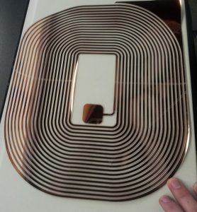
This Youtube video and the images you see demonstrate the use of an early generation of ablation laser to form circuits from flood-printed silver on polyester. This same laser has also been used to ablate copper from PET for antennas and form conductive paths on ITO/PET laminates.
There is so much room for growth in our industry. With the support of the CPEIA membership and our collaborative efforts, we have the potential to redefine how circuits are made and assembled while maintaining the advantages that define our circuits – high flexibility and eco friendly, just to name two.
Mike Streun is the President of Automation Alternatives (www.auto-alt.com). He can be reached at mstreun@auto-alt.com