
 By Nima Moghimian
Group NanoXplore Inc.
The “wonder material” of the 21st century is graphene. It conducts electricity better than copper and is much stronger and much lighter than steel. Perhaps these traits explain why it has evolved so rapidly. Graphene was discovered in 2004 and first produced in relatively large-scale in 2006. The first-generation of commercial products was released in 2008 and finally won the Nobel Prize for its inventors in 2010.
From the early days of its development, graphene was seen as a promising technology for improving functional inks and contributing to printable and flexible electronics. Some of the earliest commercial graphene products were based upon conductive inks and emerging applications including flexible sensors and antennas.
Graphene, like many other nanomaterials, possesses extraordinary properties but harnessing those properties for use in commercial products has been challenging. In 2013, the European Union created a Graphene Flagship program to promote the development of graphene, committing 1 billion euros in funding over a 10-year time frame. IDTechEx predicts a market value of about US$200 million for graphene in 2026 whereas other market analysts have suggested numbers up to $1 billion.
The types of commercial graphene
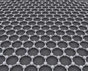
There are two major categories of commercial graphene: thin film graphene, produced by Chemical Vapor Deposition (CVD), and bulk powder graphene or few-layer graphene (FLG). FLG has properties approaching ideal graphene and can be produced in large volumes at costs acceptable to many industrial users.
CVD graphene is made by chemically depositing carbon atoms from a vapour precursor on a substrate (e.g. copper crystal) under highly controlled conditions. Such graphene is transparent and almost defect-free; but is not “freestanding” and certainly not cheap.
FLG is usually produced by mechanochemical exfoliation of graphite. Graphene made by this technique is of lower quality but much cheaper than CVD graphene and readily obtained in large volumes. Powder graphene can be easily mixed in polymer composites and has turned out to be very useful for tuning electrical, mechanical and thermal properties. However, the films obtained from FLG are not transparent and colour remains an issue.
Both CVD and FLG technologies have potential applications in printed and flexible electronics. Generally, CVD is better for electronic and photonic devices, especially where a continuous sheet of material is required. Since FLG can be added to many materials, such as polymers already used in printing and electronics, it has many potential applications. For example, it can improve the surface properties of substrates, improve the conductivity of inks, and provide innovative barrier, heat management and electromagnetic shielding properties in flexible devices and structures.
For instance, graphene-based conductive inks can easily replace conductive polymers. FLG inks with high conductivity (1-100 S/cm) have already been demonstrated. FLG inks still have lower conductivity than metal prints, but are lighter, more flexible and more processable.
Developing the next generation of graphene inks
The conversion of FLG into useful inks or coating requires careful formulation. Chemistries are needed that allow removal of the carrier resin at relatively low temperatures without deteriorating the uniformity of the printed film, and without damaging the flexible substrate. The carrier should also have suitable rheological and wetting properties, as well as carefully designed shear-response characteristics to effectively transfer the ink onto the substrate.
To address these issues, Group NanoXplore Inc. is developing the next generation of graphene inks for flexible electronics. Designed to ensure homogeneous dispersion of the graphene and ease of carrier removal, these inks enable printing integrated structures for smart packaging, for example, with high conductivity, uniformity and stability at low curing temperatures.
Lessons learned from the commercialization of carbon nanotubes, graphene’s sister material, have helped to very rapidly develop FLG manufacturing processes to industrial scale. Low-defect graphene powder with good batch to batch consistency is now being produced at industrially acceptable cost levels. FLG materials in easy-to-use product forms, such as masterbatch pellets and resin formulations, have opened the path for rapid adoption across many fields. Formulated FLG inks are starting to replace conductive polymers for printed and flexible electronics. Flexible graphene-based printable antennaes are now very close to commercialization, and more is to come.
Graphene’s unique properties have made the new wonder material’s journey from discovery to maturity much faster than that of many of its fellow nanomaterials.
Nima Moghimian, PhD, is Product Development Scientist at Group Nanoxplore Inc. (http://nanoxplore.ca) He can be reached at moghimian@nanoxplore.ca.